Introduction
The most difference between a Microcontroller(MC) and a Microprocessor(MP) is that MC uses its build-in memory and registers with running a compiled program to do certain specific work; whereas the MP is concerdered as a general-purpose processing unit that can do multi-task work according to the I/O states.
-
There is always a pre-compiled program stored in the “code segment” (AKA: .cseg) used to determine which instruction should be executed next, this part of memory would not be initiated when the hardware is reset. Usually a MC has several parallel ports that can be configuared as either output (PORTx) or input (PINx) by configuration registers (DDRx), but they are independent from each other.
-
As for a MP, the processing device uses “BUS” as the interface to communicate with external devices. This means, the MP has only one interface on it. To introduce the BUS, serial and parallel communication is the pre-requisite. In brief, the MP exchanges the data with other external I/O devices by sending and receiving the data and address via BUS. The address is bundled with the data in order to nagivate the data, just like the Program Counter (PC) and the data in RAM (.dseg).
The reason why we want to configure a Microcontroller as a Microprocessor is that we sometime need a device to attach multiple I/O devices, to execute different programs according to different occasions/scenarios (or we simply just want it easier to upgrade), or to optimize its interface. Although the MC has limited ability to handle its outside devices, but it does not require lots of additional code and devices, with the completed RISC memory model it is widely used to controll electronic signals in simple applications nonetheless.
Example
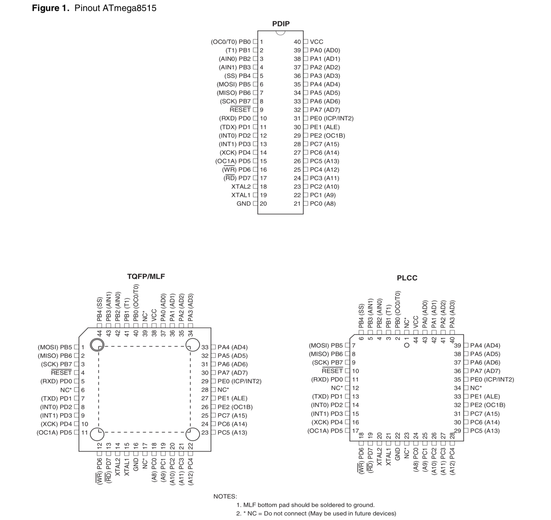
The ATmega8515 is a well-known microprocessor in AVR serie, it has 4 ports (DDRA, DDRB, DDRC, DDRD) with 8 pins on each according to the data-sheet. As a MC, we use the following commands or instructions to get access with them.
- In C language:
#include <avr/io.h>
int main (void)
{
	int dip;
	/* initialize PORTA as output and PORTD as input */
	DDRA = 0xFF;
	DDRD = 0;
	/* infinite loop of input/output combinations */
	while(1)
	{
		dip = PIND;	//get binary data from port and store in variable
		PORTA = dip;  //put variable contents to port
	}

}- In Assembly:
.cseg
/* initialize PORTA as output and PORTD as input */
init:
ldi R16, 0xFF
ld DDRA, R16
ldi R16, 0
ld DDRD, R16
/* input and output data from/to register R17 and repeat*/
pt1:
in R17, PIND
out PORTA, R17
fini:
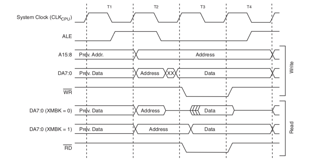
rjmp pt1In the above example, DDRA and DDRD are 8-bit I/O parallel interfaces, and they only exchange data once at a time according to the sequence in the code. Given the pinout diagram above, notive that there are AD7:AD0 and A15:8 in the brackets right beside the pins after PA and PC. And these, are also can be used as the BUS interface. To natively generate bus waveforms, a certain control register called “MCUCR” is used to switch the ATmega8515 into this mode.
- In Assembly:
/*determine the control register, data, and address*/
.EQU BUSON=$80
.EQU VAL=$A5
.EQU ADR=$1234

.cseg
/* initialize or load the values into the regs */
init_bus:
	ldi R16, BUSON
	out MCUCR, R16
	ldi R16, VAL
/* constantly output data with the same address*/
pt1:
	STS ADR, R17
fini:
	rjmp pt1
Results
The results of the program above, is that you can get “00010010” on A15:A8 and “00110100” on AD7:AD0, which is “12” and “34” in hexdecimal from measuring the falling edge of the ALE signal (consider it as the time reference), and the other part of the bus cycle at the time of raising edge of the /WR (another reference point) is “10100101”, which is “A5” in hexdecimal.
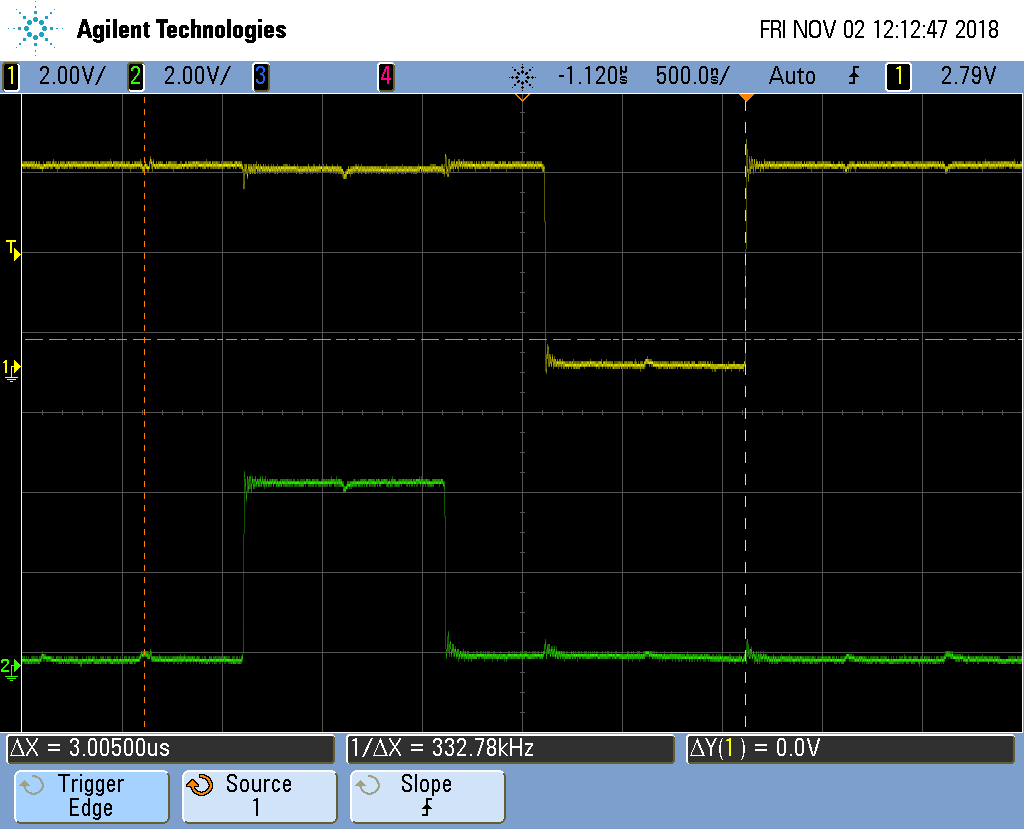
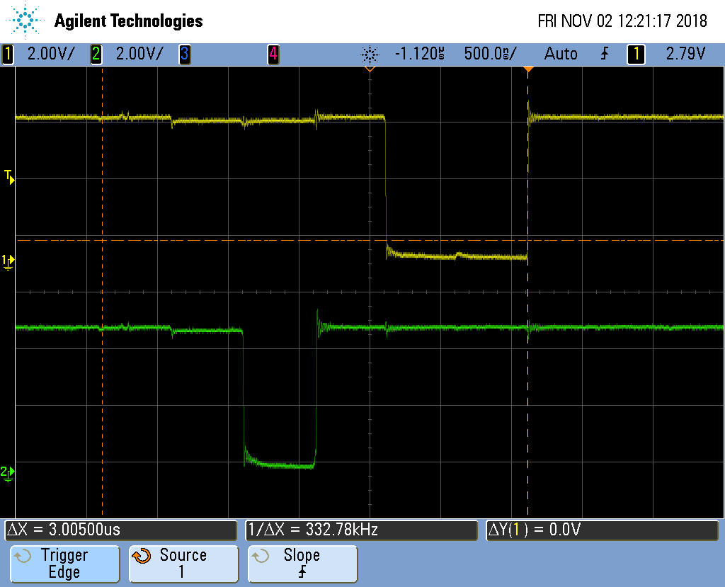
From the waveform above, we can firstly mark down the reference signals ALE and /WR, two vertical cursors indicate the period of a bus cycle, which has 6 internal clock cycle (CPU clk@1MHz). The Channel-2 in the sencond figure is data signal measured from pin AD0, notice that at the falling edge of the ALE is at “LOW” state (the LSB of ADR) and the raising edge of the /WR is at “HIGH” state (the LSB of VAL).